XC9536 Small Board

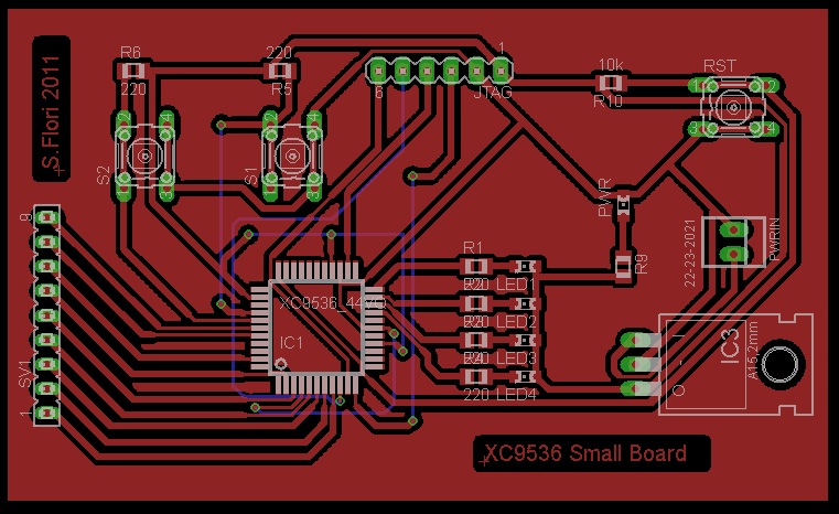
I have built a small test board expecting to a more complete system, this board was built on single-sided copper layer using the method of photoetching, where most of the components are SMT (Surface Mount Technology).

The CPLD is a Xilinx xc9536 vq44, bought for a few euro on ebay, which i support via a JTAG interface using the Xilinx ISE tool with a programmer for parallel port. The hardware description language that i use widely is Verilog, one of the two most used with the well-known VHDL.

The card mount just 4 diodes LEDs, an expansion port, a JTAG port, 2 buttons and a reset button. The clock comes from the outside through the third pin of the expansion port, to minimize clutter also because the whole thing was built and assembled very quickly just for testing cross compatibility of HW / SW around the ISE toolchain-> Programmer -> CPLD. The clock in this case is generated by a PIC16F628 mounted on a breadboard, very simple, not crucial to describe it in detail.

Coming soon i will post full details of the experimentation board, also based on the same CPLD, but with onboard clock generation using a crystal of 4 MHz, a serial EEPROM, 8 LEDs, 4 buttons plus 1 reset, 2 seven-segment display and a small external expansion port.

Here are some pictures and a video where i show the xc9536 running a program for 4-bit binary count displayed on available 4 LEDs, occasionally interrupted by a manual reset to test the proper operation of the software and hardware.

Soon other examples that also uses the two buttons and the expansion port connected to a Hitachi 44780 controller LCD display.

A video test of sequential 4-bit binary counting.

incorporato da Embedded Video

YouTube Direkt

Here is a link to the zipped file containing an EagleCad file and a pdf with good layout ready for printing on photo paper using 1:1 scale

File Eagle

Pubblicato in CPLD Xilinx | Contrassegnato , , , , , | 1 commento

NVRAM Flasher, manual NVRAM programmer

Hello everyone,
expecting to build a Z80 system, i have constructed this simple programmer for my nvram. I apologize for the circuit diagram drawn by hand, some parts may be hard to read, but it is very simple and intuitive.
The operation consists of inserting data one byte at a time, in hexadecimal, from the keyboard connected via PS2 port, the program steps sequentially and at the next (switched from zero). Once you have finished entering all the bytes you want, by pressing the escape button, the programmer enters reading-mode from location 0 and then hitting Enter you should see the following addresses sequentially and the data they contain.
The board also features a port for debugging and program the PIC via ICD using mikroC PRO for PIC.
Here come some pictures and sources (the project) for that compiler, if you want you can adapt to other software, another pic, etc. … you can modify to your liking, everything is still under development, although it works, but i would also include the possibility of random access to data and also the expansion for the selection of addresses using 2 CMOS CD4040 counters.

Schematic (click to zoom):

Pictures and sources (click to zoom).

Software sources

Pubblicato in PIC Microchip® | Contrassegnato , , , , , , | Lascia un commento

USB & PIC experiments, Protocollo USB con PIC e Microsoft Windows

Hi, these days I did some testing for the management, through the USB protocol, of a stream of data to a PIC18F2550, using an HID class device firmware and VisualC # as a language for the application on Windows, and i wanted to publish my work (more than a week working on).
We start from the hardware configuration that i made on breadboard, it is standard pattern for this type of applications, which can be expanded at will of the designer (the pattern is a classic pattern taken from the web, nothing innovative):

I have attached a series of 8 LEDs with 220 Ohm resistors on PORTB and LEDs on the port that flashes when the USB is recognized by Windows. The firmware that i did, as HID class, can be modified at will to determine how big the buffer must be read and write via USB, and to give a unique identification code so that it is not confused with other USB devices connected to the PC, this code is given by the pair VID and PID (Vendor ID and Product ID), which in my case i chose 1234 and 0001 (in hex). Written and compiled the HID descriptor, coupled to the main(), or what determines what to do when they get data from USB, you have to program the PIC18F2550. Hex is available in the source that i provides.
The first time you connect the hardware inside the FW just mentioned, Windows will install automatically HID (Human Interface Device) which can be seen between devices (resource management), assigned with your own VID and PID.

We now have the hardware connected and recognized, not just open the door of communication via the USB HID class with a programming language of your choice, i typically use the C or Basic, essentially, but because i want a nice view interface  i use VisualC # (via the programming of Windows Forms).
The program i wrote is very simply: you connect the device with VID and PID 1234 and 0001, and once connected you can send a byte to the PIC via USB typing data in a box, in decimal, and pressing SEND.
This is the first step to communicate from one application to win out on a device interfaced to the USB, everything has been written by hand, FW and SW, and so we have full control (or almost) of everything happens and what can not work.
Here is an issue on which i spend some time, but not much yet.
To properly write the firmware (written in C) on the PIC, through any programmer, you must properly configure the configuration bits of the microcontroller. The PIC that i have chosen have this internal structure block (as you note is a page of datasheet from Microchip ®, please read it for more detail):

We need to set the behavior of the multiplexer according to our oscillator, i chosen a crystal of 4 MHz, then the correct settings (found after several trials) are these:

  • 96 MHz PLL prescaler : No Divide (4 MHz input)
  • CPU System Clock Postscaler: [OSC1/OSC2 Src: /1][96MHz PLL Src: /2]
  • Full-Speed USB Clock Source Selection: Clock src from OSC1/OSC2
  • Oscillator: XT: USB-XT

It ‘s very important to use XT oscillator and NOT HS if we use a crystal, and also that the USB works at 48 MHz, as we are doing now, in fact signed by the multiplexer with selection USBDIV is coming out exactly a frequency of 48 MHz, half of that generated by the internal PLL.
If these paths are not set up correctly with the internal configuration bit, windows does not recognize anything, placing doubts over the entire system, will the FW I’ve written correct? HW will be wrong some connection? … probably not been set correctly these configuration bits.
Last thing very important and quite critical, due to many failures, is the capacitor on VUSB of 220nF, the value is not critical, but criticism is its lack.
Now let’s see some pictures of HW and then a video of the operation:

I’ll give you the source of the firmware, also you will find the . hex ready for those wishing to try

FW Sources

Here are the sources in VisualC # application that communicates with the device, will find the sources and also the little program already compiled in executable format:

HID Sources (Visual C)

Executable (.exe)

If you want you can try to read some source, modify it, recompile it for other PICs, for example, 18F4550, and if you try even if the exe will run properly with your HW / FW, use other ports of the PIC, have them do other things (instead to view the status with the 8 LEDs), everything is editable and customizable.
As you may have noticed i have not made a pcb as this trial is not definitive but is a pattern seen more as a “testbench” for various uses, attempts to work at an hardware and software interfaced to the USB device under the operating system Microsoft Windows.
All the real work was to understand how the bytes are sent via USB from a Windows application to a digital port of a MCU, so most of the time was used to fully understand how to write the HID firmware and run it with all the real problems encountered as settings, frequency, fuses … etc. ..
I hope it was to your liking.

Pubblicato in PIC Microchip® | Contrassegnato , , , , , , , , | 1 commento

AM Receiver

AM Receiver with a FET

This project was created with the aim of creating a very simple receiver to hear the AM modulation of the CB in my town. It is not a recent creation, is a couple of years old , but recently i picked up from the drawer of the “memories”.

My receiver can, in theory, cover the range between 16 and 30 MHz, using an active FET BF245. This is a classic pattern of reaction receiver, carried out through retroactive part of the signal routed to the gate of the FET through the tuning circuit consisting of L2, C1 and the varicap diode DV1. The amount of reaction, upon which the sensitivity of the system, is determined by potentiometer R5. If you exceed in that regulation of reaction, the receiver will come under the self-oscillation, so you have to training your ear, is a matter of habit in use such of these receivers, which are well attuned to the adjustment of the reaction.

We notice that they are self oscillatory regime when through the headphones you hear a whistle that covers all possible received signals.

The line is controlled by the varicap DV1, and adjusted by varying the voltage applied to it using the potentiometer R3.

The low-frequency output is taken through the electrolytic capacitor C5 (a tantalum would be perfect), after filtering the high frequency components through C4. Of course, as you can see, the level of the output signal is too low to be heard directly in the headphone or speaker, but just any preamplifier with high input impedance and a small glides, TDAxxxx for example, to listen in speaker. For my tests i used the mic input of my stereo system, and the clarity of the signal was discrete, reminding us that the receiver is still very simple.

The construction of the coils L1/L2, to wrap up over ferromagnetic core, is a crucial part of the project. In fact the only action on the tuning knob us to vary the bandwidth up to 6-7MHz, not making us cover the entire band from 16 MHz to 30 MHz for this fact is necessary to calibrate the ferromagnetic core, with an anti-inductive screwdriver, so that we can focus our band of interest, if the lower (16 to 23 MHz) or upper (23 – 30 MHz). The coil L2 is formed by 12 turns of enamelled copper wire of 0.5 – 0.6 mm in diameter up to a base with a core of 6 mm in diameter, taking a grip in the fourth coil to ground. The coil L1 is wound with 4 turns of the same wire, on the same media, from the “cold” L2 side, also called ground side.

Connect an antenna to receive signals in OC, possibly adjusted to the wavelength, or a stub, the old gang that has been chosen to receive. For example if I want to receive from 23 – 30MHz, choose a dipole receiver for 26-27 MHz with an appropriate length of wire should also receive something, but I have not personally tried.

When you turn on your receiver, you sling the potentiometer of the reaction, and is always kept on the limit of self-oscillation, this is indeed the point of maximum sensitivity of the receiver, but is also relatively complicated to keep exactly to the limit of self-oscillation. With some practice it will not be hard to use it.


Pubblicato in Analogic | Contrassegnato , , , , , , , , , | 7 commenti